Professor Furui Tan's group from Henan University collaborated with Professor Makhsud I. Saidaminov’ group from the University of Victoria to publish their latest research findings in Nature Communications
Nature Communications
Professor Furui Tan’s team from the School of Future Technology (Henan Key Laboratory of Quantum Materials and Quantum Energy) at Henan University and his distinguished collaborator, Professor Makhsud I. Saidaminov’s team from the University of Victoria in Canada, have recently made significant progress in convenient preparation and fabrication of metal halide perovskite thin films, solar cells and photovoltaic modules. Their research article, titled "Marker Pen Writing of Perovskite Solar Modules," has been published in the journal Nature Communications.
Commercialization of metal halide perovskite solar cells (PSCs) and other perovskite devices critically depends on the ability to cost-effectively scale the fabrication of high-quality perovskite films. Currently, spin coating is the most common method for depositing perovskite film in laboratories due to its ease of operation, low equipment cost, and good reproducibility. However, achieving a homogeneous film over a large substrate is challenging because of uneven centrifugal force, leading to substantial waste (>90 %) of the precursor ink. For large-area film coating, several industrial processing techniques like blade coating, slot-die coating, and spray coating have been studied. Despite offering good scalability and module performance, they have limitations, including unportable equipment, cumbersome alignment/calibration steps, durative labor maintenance, poor substrate compatibility for some of them, and non-uniform deposition caused by the easy aggregation of perovskite colloidal particles. For fabrication of perovskite solar modules (PSMs), additional scribing steps, referred to as P1, P2, and P3 scribing, are involved to divide a large-area device into small-area sub-cells and establish electrical interconnection in series. These scribes are typically conducted using lasers and/or mask plates, demanding high-cost facilities and precise lithography design. The process also requires substantial optimization of laser conditions, including wavelength, power, repetition rate, scribing speed, and overlap between pulses. Moreover, perovskites, in contrast to many photovoltaic materials, exhibit heightened thermal sensitivity, leading to partial degradation or redeposition in the vicinity of the laser scribe.
The research team develops a marker pen writing (MPW) process for the fabrication of PSCs and PSMs. By using marker pens, they demonstrate that not only can colloidal sizes be homogenized and stabilized, but also the films’ thickness and area can be tuned from one hundred nanometers to one micrometer and from 1 cm2 to 100+ cm2, respectively, meeting the requirements for the active layer in diverse perovskite photovoltaic devices. An ambient writing of annealing-free perovskite film is also demonstrated by engineering the precursor solvent mixture, promoting the practicality of this method. The rigid and flexible written C-PSCs exhibit the champion efficiencies of 20.4% and 19.0% under annealing conditions, respectively; 18.0% and 16.4% under annealing-free conditions, respectively. Additionally, they realize the rigid and flexible carbon-electrode modules with efficiencies of 16.3% and 14.5%, respectively, both written in a mask- and laser-free manner, showcase the large-area self-patterning capabilities of this method. Furthermore, this technology offers a convenient and rapid route for manufacturing lightweight and deformable power sources, which have been proven to drive portable and/or wearable electronic products like hygrothermographs, smart wristbands, and mobile phones. ITO- and annealing-free PSMs on elastomers and paper, as well as irregular modules of biomimetic solar leaves with balanced art and technology, can also be handwritten with marker pens. The marker pen writing is of low cost, easy patterning, large area, and suitable for on-demand deposition, making it possible to bring perovskite photovoltaics to more scenarios and enter households.
Associate Professor Dr. Chen Dong and a master's degree graduate student, Yuhao Song from Henan University in China, lead this MPW work. Professor Furui Tan from Henan University and Professor Makhsud I. Saidaminov from the University of Victoria are the co-corresponding authors. The research was supported by the National Natural Science Foundation and others.
Dr. Tan’s team is mainly engaged in studies on metal halide perovskite and organic solar cells, supercapacitors, and photodetectors. The team has published more than 50 SCI-indexed highly impact papers, with a total citation of over 2500 times. In the exploration of new energy materials, this team has pioneered and promoted the research on the carbon electrode perovskite solar cells and low-cost furan-based organic solar cells.
Dr. Saidaminov’s team from the University of Victoria in Canada is engaged in the development of conventional and next-generation semiconductors for applications in solar cells and X-ray detectors.
Link to the paper: https://www.nature.com/articles/s41467-025-61459-w
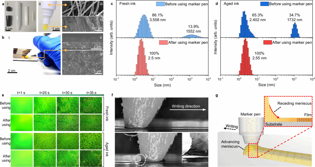
Fig. 1: Marker pen writing of perovskite films. a (i, ii) Photo of marker pen and scanning electron microscopy (SEM) image of (iii) its core and (iv) tip. b (i) Photo capturing the process of handwriting MAPbI3 perovskite films on a rigid substrate and (ii, iii) SEM images of the resultant perovskite film. c, d Dynamic light scattering (DLS) particle size analysis in fresh and aged precursor inks before and after using marker pens. e In situ microscopy photographs of nucleation evolution of fresh and aged precursor inks before and after using marker pens. f In-situ microscopy images of writing dynamics. g Schematic diagram of working principle of the MPW method.
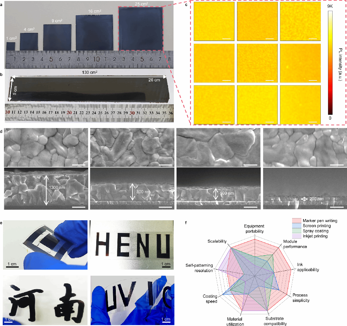
Fig. 2: Large-area and pattern engineering of perovskite films by MPW. a Photographs of the handwritten perovskite films of different areas (1–25 cm2). b Photograph of a 130 cm2 handwritten perovskite film. c PL mapping of 9 parts of a handwritten 5 cm × 5 cm perovskite film. The scale bar represents a length of 100 μm. d Top-view and cross-section SEM images of handwritten perovskite films with different thicknesses obtained by adjusting ink concentration. The scale bar represents a length of 500 μm. e Patterned perovskite films written on flexible ITO/PET substrates, constituting square, square ring, HENU (stands for Henan University), UVIC (stands for University of Victoria), and Chinese characters. f Comparison of solution-based fabrication methods for patternable perovskite films (more details in Supplementary Table 1).
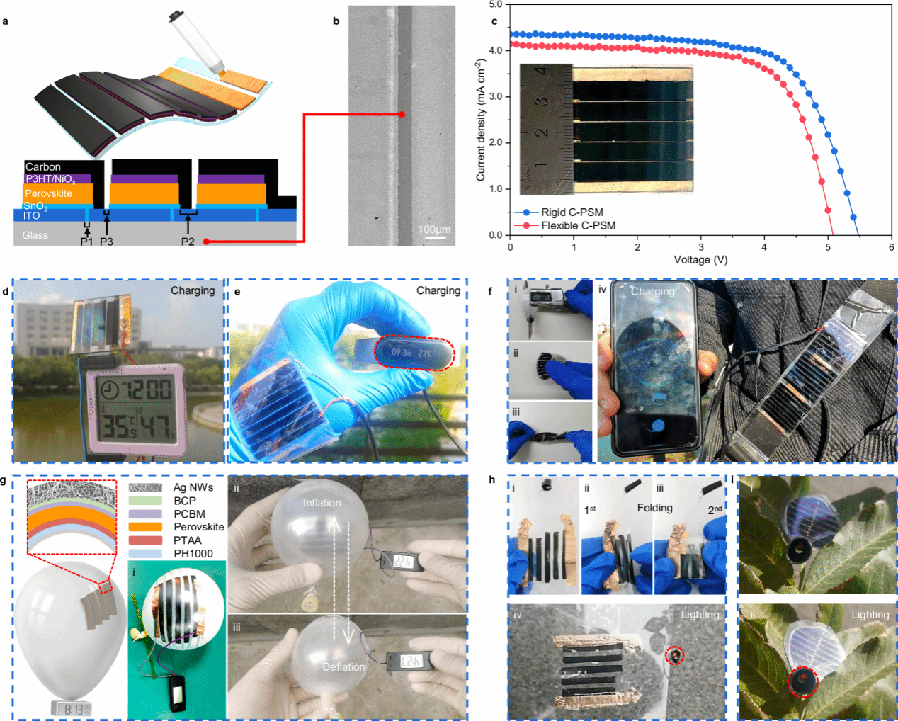
Fig. 3: Performance and applications of carbon-electrode perovskite solar modules (C-PSMs) by MPW. a Schematic of preparing C-PSM by MPW and module architecture. b Minimized distance (P2) between perovskite films written by marker pen. c Champion J-V curves of rigid and flexible annealed 4 cm × 4 cm C-PSMs (inset: photograph of the rigid C-PSM). d Demonstration of handwritten C-PSMs as power sources to drive the hygrothermograph. e Demonstration of flexible C-PSMs as wearable power sources to charge a smart wristband. f Demonstration of (i) foldability, (ii) bendability, (iii) twistability of flexible C-PSMs, and (iv) their application as wearable power sources for a mobile phone. g Demonstration of handwritten ITO- and annealing-free PSMs on (i) rubber balloons, with the sub-cell configuration of PH1000/PTAA/perovskite/PCBM/BCP/Ag nanowires (NWs), and their application as power sources for an electronic watch under (ii) inflation and (iii) deflation conditions. h Demonstration of handwritten ITO- and annealing-free PSMs on (i) cellophane paper, (ii, iii) their foldability, and (iv) their application as power sources for a light-emitting diode (LED). i Biomimetic solar leaf handwritten by marker pen and its practical application as the power source for an LED under (i) tree shade and (ii) illumination conditions.